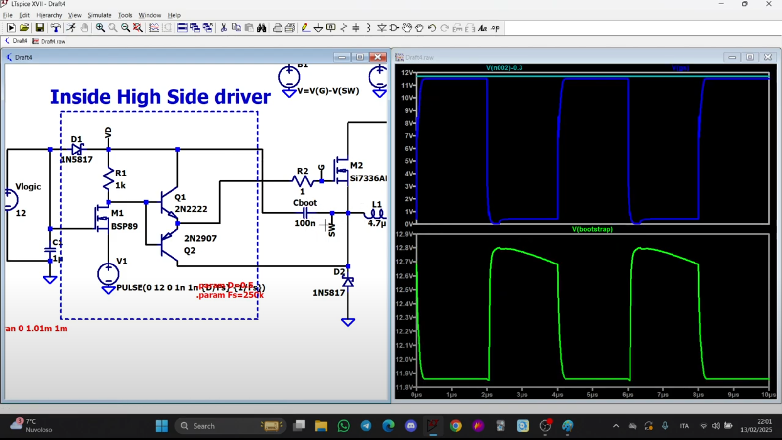

A high-side N-channel MOSFET creates one of those wonderfully inconvenient engineering problems: its source voltage moves. When the MOSFET turns on, its source may rise almost to the DC bus voltage, so a gate signal referenced to ground is no longer useful. The gate must remain several volts above the moving source, not merely above ground.
A bootstrap gate-drive circuit solves this problem with a diode, a capacitor, and some carefully timed switching. It is inexpensive, efficient, and common in buck converters, motor drives, half bridges, full bridges, inverters, and Class-D amplifiers. It is also easy to simulate incorrectly. LTspice will happily produce beautiful waveforms for a circuit that could never recharge its bootstrap capacitor in real life. Computers are very supportive that way.
This guide explains how to build a meaningful high-side bootstrap simulation in LTspice, choose realistic component values, interpret floating-node waveforms, and expose problems involving duty cycle, startup, undervoltage lockout, dead time, parasitics, and switch-node undershoot.
What a High-Side Bootstrap Circuit Actually Does
A standard half bridge contains a high-side MOSFET between the positive bus and the switch node, plus a low-side MOSFET between the switch node and ground. Both devices are often N-channel MOSFETs because they generally provide better conduction performance than comparable P-channel parts.
The low-side MOSFET is straightforward to drive because its source is connected to ground. A 10- or 12-volt gate signal referenced to ground produces approximately the same gate-to-source voltage.
The high-side MOSFET is different. Suppose the bus is 48 volts and the desired gate-to-source voltage is 10 volts. When the switch node rises to 48 volts, the high-side gate must rise to roughly 58 volts. The driver therefore needs a floating power supply that rides on top of the switch node.
A typical bootstrap network contains:
- A bootstrap capacitor connected between the driver’s floating supply node, commonly labeled VB or HB, and the switch node, commonly labeled VS, HS, or SW.
- A bootstrap diode connected from the low-voltage driver supply to VB.
- An optional series resistor that limits charging current.
- A local bypass capacitor across the gate-driver supply.
When the low-side MOSFET conducts, the switch node is pulled near ground. Current then flows from the driver supply through the bootstrap diode and charges the bootstrap capacitor. When the high-side MOSFET turns on, the switch node rises toward the bus voltage. The charged capacitor rises with it, maintaining a floating voltage between VB and VS that powers the high-side driver. Official application notes from Texas Instruments, STMicroelectronics, Microchip, and onsemi describe the same two-phase charging and discharging process.
Why LTspice Is Useful for Bootstrap Design
Hand calculations are essential, but they usually examine a simplified worst case. LTspice lets you watch the bootstrap voltage change during startup, switching transitions, high-duty-cycle operation, load-current reversals, and abnormal conditions.
A useful simulation can answer questions such as:
- Does the bootstrap capacitor charge before the first high-side pulse?
- How far does the floating supply droop during the high-side on-time?
- Does VB-to-VS remain above the driver’s undervoltage lockout threshold?
- Is the low-side interval long enough to recharge the capacitor?
- How much peak current flows through the bootstrap diode?
- Does switch-node undershoot overcharge the capacitor or violate driver limits?
- Are the high-side and low-side MOSFETs ever on simultaneously?
LTspice includes a schematic editor, transient simulator, component models, and an integrated waveform viewer. It also supports differential voltage measurements, which are critical when examining a floating high-side driver.
Building the Half-Bridge Model in LTspice
1. Start With the Power Stage
Create a DC bus source and connect two N-channel MOSFETs as a half bridge. The drain of the high-side device connects to the bus, its source connects to the switch node, and the low-side device connects between the switch node and ground.
Add a realistic load. For a buck converter, use an inductor, output capacitor, and resistance. For a motor-drive test, an inductive load with winding resistance is more meaningful than a lone resistor. Load current affects when the switch node reaches ground and whether the bootstrap diode can conduct.
2. Add a Gate-Driver Model
The best starting point is the manufacturer’s LTspice-compatible macromodel for the intended half-bridge driver. A realistic model may include propagation delay, output resistance, undervoltage lockout, dead-time behavior, supply current, and logic thresholds.
When no model is available, create a functional model using voltage-controlled switches or behavioral voltage sources. Include at least:
- A low-side output referenced to ground.
- A high-side output referenced to VS.
- Finite output resistance.
- High-side supply current.
- A simplified undervoltage lockout threshold.
- Propagation delay and nonzero rise and fall times.
Do not assume that a generic ideal voltage source represents a gate driver accurately. A zero-ohm source can charge the MOSFET gate instantaneously, conceal gate-current demand, and turn a serious switching problem into a very tidy fairy tale. LTspice also supports importing third-party MOSFET and subcircuit models when the pin order and symbol attributes are assigned correctly.
3. Connect the Bootstrap Components
Connect the bootstrap capacitor from VB to VS. Connect the diode from the driver’s VCC supply toward VB, with its cathode at VB. If a charging resistor is used, place it in series with the diode.
Add a bypass capacitor from VCC to ground near the simulated driver. Without it, the bootstrap charging pulse may pull VCC downward unrealistically or force an ideal voltage source to deliver infinite peak current.
4. Generate Complementary PWM Signals
Use two pulse sources, behavioral sources, or piecewise-linear sources to create complementary high-side and low-side commands. Include dead time between transitions. For example, at 100 kHz, a period is 10 microseconds. A 100-nanosecond dead-time interval can be inserted after one MOSFET turns off and before the other turns on.
Never begin by using perfectly complementary signals with zero delay. Real MOSFETs and drivers need time to discharge gate charge. Zero dead time can produce shoot-through, while excessive dead time increases body-diode conduction and may alter bootstrap charging.
Sizing the Bootstrap Capacitor
The basic sizing relationship is:
CBOOT >= QTOTAL / ΔVBOOT
Here, QTOTAL is the total charge removed during the longest high-side on-time, and ΔVBOOT is the maximum acceptable droop in the floating supply.
Total charge should include more than the MOSFET’s headline gate-charge value:
QTOTAL = QG + QLEVEL_SHIFT + (IQBS + ILEAK + IGSR) × TON
The terms may include MOSFET gate charge, internal level-shifter charge, high-side driver quiescent current, diode leakage, capacitor leakage, MOSFET gate leakage, and current through a gate-to-source resistor. Gate charge often causes an immediate voltage step, while quiescent and leakage currents create a gradual slope during the high-side pulse.
Worked 48-Volt Example
Consider a 48-volt half bridge operating at 100 kHz with an 80% maximum high-side duty cycle. Assume:
- MOSFET gate charge: 60 nC
- High-side driver current: 200 µA
- Combined leakage allowance: 20 µA
- Internal level-shift charge and margin: 5 nC
- Maximum high-side on-time: 8 µs
- Allowed bootstrap droop: 0.5 V
The time-dependent charge is approximately:
(200 µA + 20 µA) × 8 µs = 1.76 nC
Total charge is therefore:
QTOTAL = 60 nC + 5 nC + 1.76 nC = 66.76 nC
The calculated minimum capacitance is:
CBOOT = 66.76 nC / 0.5 V = 133.52 nF
A designer might begin with a nominal 220 nF ceramic capacitor, then verify its effective capacitance at the applied bias voltage and temperature. A 470 nF part may provide greater droop margin, but larger is not automatically better. More capacitance requires more charging current and more time to recharge.
Ceramic capacitors can lose a significant portion of their nominal capacitance under DC bias. The simulation should therefore test the estimated effective value, not only the number printed on the package. Vendor guidance also recommends preserving adequate margin for temperature, tolerance, and voltage-dependent capacitance.
Choosing the Bootstrap Diode and Resistor
The bootstrap diode must withstand approximately the bus voltage when the switch node is high, plus transient margin. In a 48-volt system, a 100-volt-rated diode may be appropriate, depending on ringing and operating requirements. Higher-voltage motor drives may require several hundred volts of reverse-voltage capability.
Important diode characteristics include:
- Reverse-voltage rating
- Forward-voltage drop
- Reverse-recovery charge
- Leakage current at temperature
- Peak and average charging current
A Schottky diode offers low forward voltage and negligible reverse recovery at suitable voltage ratings. Fast-recovery silicon diodes are common at higher bus voltages. The diode should be modeled with junction capacitance, leakage, and recovery behavior when switching losses or ringing matter. Vishay and other power-semiconductor manufacturers emphasize matching bootstrap diodes to the driver voltage, switching frequency, and transient stress.
A series resistor limits the charging-current spike and can reduce ringing. However, too much resistance slows charging and creates additional voltage loss. Sweep values such as 0, 2.2, 4.7, and 10 ohms while monitoring the minimum bootstrap voltage and diode peak current.
Waveforms You Should Always Plot
Bootstrap Voltage
Plot V(VB,VS), not merely V(VB). This differential trace is the actual floating supply voltage seen by the high-side driver.
High-Side Gate-to-Source Voltage
Plot V(HO,VS). Plotting HO relative to ground can be misleading because HO may rise to the bus voltage plus the gate-drive voltage. A 58-volt HO waveform in a 48-volt converter is not evidence that the MOSFET gate is being abused; the relevant measurement may still be only 10 volts from gate to source.
Switch-Node Voltage
Plot V(VS) and inspect overshoot, undershoot, ringing, rise time, and fall time. A negative VS transient can momentarily increase the bootstrap voltage and stress the driver’s floating pins.
Bootstrap-Diode Current
Plot the diode current during each recharge interval. A narrow pulse can have a surprisingly high peak value, especially with an ideal supply, ideal diode, zero series resistance, and large capacitor.
Both MOSFET Gate Voltages
Display high-side and low-side VGS traces together. They should not overlap above their meaningful turn-on thresholds. This is a better shoot-through check than merely comparing the logic input signals.
LTspice permits ground-referenced and differential traces directly in the waveform viewer, so floating voltages should be evaluated in their proper reference frame.
Useful LTspice Commands and Parameter Sweeps
A transient command might resemble:
The stop time should cover startup plus enough switching cycles to reach repeatable operation. The maximum timestep must be small enough to resolve gate transitions, diode-current spikes, and dead time.
Parameter sweeps make the design much more informative:
Useful automated measurements include:
Run additional sweeps for supply voltage, switching frequency, duty cycle, temperature, load current, MOSFET model, and driver-current consumption. Worst-case behavior rarely occurs at the friendly nominal condition highlighted in the product brochure.
Common Simulation Problems
The High-Side Output Never Turns On
The bootstrap capacitor may not have an initial charging opportunity. Begin with the low-side MOSFET conducting briefly, add a startup sequence, or verify that load current pulls VS low enough to forward-bias the bootstrap diode.
The Simulation Works at 100% Duty Cycle
A simple bootstrap supply cannot support indefinite high-side on-time because the capacitor eventually discharges. A model that works forever at 100% duty cycle probably omits high-side supply current, leakage, UVLO, or all three. Static high-side operation generally requires a charge pump, isolated bias supply, or another continuously powered floating supply.
Bootstrap Voltage Is Unrealistically Perfect
Ideal capacitors have no ESR, no leakage, no voltage coefficient, and no temperature drift. Ideal diodes have no recovery charge. Add realistic models or explicit parasitic elements before trusting the result.
LTspice Reports “Time Step Too Small”
Perfect switches, zero-resistance loops, abrupt behavioral expressions, and ideal inductors can create numerical trouble. Add small realistic resistances, finite transition times, capacitor ESR, and inductor winding resistance. Initial conditions may help diagnose a problem, but they should not be used to hide a startup failure.
The Gate Waveform Looks Far Too High
You are probably measuring the high-side gate relative to ground. Measure gate to source. Floating circuits are not difficult once every voltage is referenced correctly; they are merely skilled at looking guilty.
Practical Experience: Lessons From Realistic LTspice Work
The following field-style lessons reflect recurring experiences encountered when constructing and reviewing high-side bootstrap simulations.
Build the Model in Layers
The most reliable workflow is to begin with a deliberately simple circuit. First test the half bridge with ideal gate commands and confirm that the power stage behaves correctly. Next add realistic MOSFET models. Then add the gate-driver model, bootstrap network, dead time, parasitic inductance, and abnormal operating cases.
Adding everything at once makes debugging unnecessarily dramatic. When the simulation fails, there may be twenty possible causes: a reversed diode, incorrect subcircuit pin order, missing ground, UVLO activation, overlapping PWM, floating logic input, unsuitable timestep, or a MOSFET model that expects a different symbol.
Layered construction turns the process into a sequence of small questions. Does the switch node move? Does the capacitor charge? Does the driver see enough VB-to-VS voltage? Does the gate rise relative to its source? Small questions are much less likely to consume an entire afternoon.
Test Startup Separately From Steady State
A circuit can operate perfectly after the bootstrap capacitor is charged while failing completely during its first few microseconds. One common mistake is beginning the simulation with a high-side pulse before the switch node has been pulled low. A sophisticated driver model may correctly block the pulse because the floating supply is below UVLO.
Create a startup test in which the low side receives one or more charging pulses before normal PWM begins. Then create a harsher test with the controller requesting high-side conduction immediately. The second test reveals whether the real system needs precharge logic, a startup delay, or guaranteed low-side activity.
Use Worst-Case On-Time, Not Average Duty Cycle
Average duty cycle can be deceptive in motor-control and inverter applications. A modulation algorithm may occasionally hold one high-side device on much longer than the average value suggests. At low electrical frequency, certain commutation states can leave a bootstrap capacitor without a convenient recharge interval.
Sweep the maximum uninterrupted high-side on-time directly. Watch the bootstrap voltage slope and compare its minimum value with the driver’s worst-case UVLO falling threshold. Include gate-charge variation, hot leakage, low VCC, diode drop, and reduced ceramic capacitance. Nominal simulations are reassuring; corner simulations are useful.
Pay Attention to Negative Switch-Node Spikes
Once package and PCB inductance are added, VS may dip below ground during commutation. That negative excursion can briefly forward-bias internal structures, increase the effective bootstrap charging voltage, or violate the driver’s allowed negative-transient specifications.
Add a few nanohenries of common-source, drain-loop, and interconnect inductance rather than assuming every wire is perfect. The resulting ringing may look less attractive, but it is far more informative. It also explains why physical layout, Kelvin source connections, gate-loop area, and local decoupling matter even when the schematic is flawless.
Compare Simulation Results With Charge Accounting
After a transient run, estimate the expected voltage drop using ΔV = Q/C. If a 60 nC gate is supplied by a 220 nF effective bootstrap capacitor, the immediate theoretical drop is roughly 0.27 volts before quiescent-current effects. If LTspice reports almost no drop, inspect the driver model and capacitor value. If it reports several volts, investigate unexpected current paths.
This quick comparison catches modeling errors faster than staring at twelve colorful traces. Simulation is most powerful when it works beside first-principles calculations rather than replacing them.
Keep a Simplified and a Detailed Version
A simplified functional model runs quickly and is excellent for sweeping capacitance, duty cycle, frequency, and timing. A detailed model containing nonlinear MOSFET capacitance, reverse recovery, package inductance, and driver internals may run much more slowly but provides better transition-level insight.
Maintaining both versions is practical. Use the simple model to explore the design space, then use the detailed model to validate the most important operating points. Asking a massive nonlinear model to perform hundreds of parameter combinations is a fine way to turn a fast computer into a decorative heater.
Conclusion
Simulating a high-side bootstrap circuit in LTspice is not merely a matter of placing a diode and capacitor beside a half bridge. A trustworthy model must represent the floating reference, gate charge, high-side supply current, recharge interval, diode behavior, dead time, UVLO margin, and power-stage parasitics.
The most important waveforms are differential: VB-to-VS for the bootstrap supply and HO-to-VS for the high-side gate voltage. Test startup, maximum high-side on-time, minimum supply voltage, temperature-sensitive leakage, reduced ceramic capacitance, negative switch-node transients, and the full range of load-current directions.
When the simulation agrees with charge-based calculations and remains stable across realistic corner cases, it becomes a valuable design tool rather than an electronic confidence generator.