
Laser cutting solder stencils may not sound like the most glamorous topic in electronics manufacturing, but ask any PCB assembler what can ruin a perfectly good production day, and solder paste problems will stroll into the room wearing muddy boots. A solder stencil is the quiet hero of surface-mount technology: a thin, precisely cut sheet that controls where solder paste lands, how much paste gets deposited, and whether your tiny components sit politely on their pads or drift around like they are auditioning for a soap opera.
In modern PCB assembly, especially with fine-pitch ICs, QFNs, BGAs, and compact IoT boards, a laser cut solder stencil is often the difference between repeatable manufacturing and a troubleshooting marathon. The laser cutting process creates accurate apertures that match the PCB paste layer, helping manufacturers apply solder paste consistently before component placement and reflow. When done correctly, it improves solder joint quality, reduces bridging, minimizes tombstoning, and saves engineers from muttering things at midnight that should not be printed on a datasheet.
This guide explains how laser cutting solder stencils works, why it matters, what materials and thicknesses are commonly used, and how stencil design decisions affect real assembly results.
What Is a Laser Cut Solder Stencil?
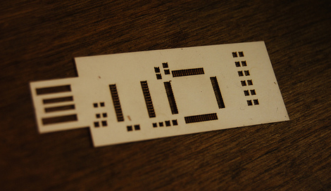
A laser cut solder stencil is a thin sheet, usually stainless steel, with precisely cut openings called apertures. These apertures align with the surface-mount pads on a printed circuit board. During solder paste printing, a squeegee spreads solder paste across the stencil. Paste passes through the apertures and lands on the PCB pads. The stencil is then lifted away, leaving controlled paste deposits ready for pick-and-place assembly.
The phrase “laser cut” matters because the cutting method affects aperture accuracy, wall smoothness, paste release, and repeatability. Older or lower-cost approaches, such as chemically etched stencils or DIY plastic films, can work in certain prototype situations. However, for fine-pitch components and production runs, laser cutting offers tighter control and cleaner geometry.
Why solder paste control is so important
Solder paste is not just shiny gray frosting for circuit boards. It contains solder alloy particles suspended in flux, and it must be deposited in the right amount. Too little paste can cause weak joints, opens, or poor mechanical strength. Too much paste can cause bridging, solder balls, floating components, or short circuits. The stencil is the measuring cup, cookie cutter, and traffic cop all at once.
In surface-mount assembly, the stencil determines paste volume through three main factors: aperture size, aperture shape, and stencil thickness. Laser cutting makes it possible to control those details with high precision, which is especially valuable when components are small enough to make a grain of rice look like patio furniture.
How Laser Cutting Solder Stencils Works
The process begins with the PCB paste layer, usually exported as Gerber data from PCB design software. This paste layer defines where solder paste should be printed. The stencil manufacturer reviews the data, applies any requested aperture modifications, and then uses a laser system to cut the openings into metal foil.
Step 1: Gerber file preparation
Most PCB design tools generate separate top paste and bottom paste files. These files are not the same as copper layers or solder mask layers. The paste layer tells the stencil maker exactly where the apertures should go. For a single-sided assembly, only one stencil may be needed. For double-sided SMT assembly, separate top and bottom stencils are usually required.
Good file preparation includes checking component footprints, confirming pad sizes, removing paste openings from test pads or vias that should not receive paste, and reviewing thermal pad patterns. A stencil can only cut what the data asks for, so if the paste layer contains nonsense, the laser will faithfully produce precision nonsense. Technology is obedient like that.
Step 2: Laser cutting the apertures
During laser cutting, a focused beam cuts each aperture into the stencil foil. Stainless steel is the most common material because it is durable, stable, and suitable for repeated printing. The laser can create small, repeatable apertures for fine-pitch components, and it can follow custom geometries such as home-plate shapes, rounded rectangles, windowpane thermal pads, or reduced apertures for special packages.
Laser cutting typically produces more vertical aperture walls than chemical etching. This helps maintain consistent paste volume. For many SMT applications, especially dense boards, that consistency is a major reason laser cut solder stencils have become the standard choice.
Step 3: Finishing and polishing
After cutting, many high-quality stencils are electropolished, chemically polished, or coated to improve paste release. Electropolishing smooths the aperture walls, making it easier for solder paste to separate from the stencil during lift-off. Some manufacturers also offer nano coatings or surface treatments that reduce paste adhesion, improve cleaning performance, and support finer apertures.
For very small components, smooth aperture walls are not a luxury. They are part of the recipe. If paste clings to the aperture wall instead of transferring cleanly to the pad, deposits become inconsistent, and assembly defects begin waving from across the room.
Common Materials Used for Solder Stencils
Laser cut solder stencils are most commonly made from stainless steel, but other materials exist for specific use cases.
Stainless steel stencils
Stainless steel is the industry favorite because it offers strength, dimensional stability, and good wear resistance. It handles repeated printing cycles well and supports accurate laser cutting. For professional SMT assembly, stainless steel is usually the default choice.
Nickel and electroformed stencils
Electroformed nickel stencils are often used for demanding fine-pitch applications where excellent paste release is needed. They can offer very smooth aperture walls and high durability, though they are typically more expensive than standard laser cut stainless steel stencils.
Polyimide and Mylar prototype stencils
For hobbyists or very early prototypes, laser cut polyimide, Mylar, or Kapton-style film stencils can be useful. They are affordable and easy to handle, especially for small boards. However, they are less durable, less dimensionally stable, and generally not ideal for high-volume or fine-pitch production. They are the “good enough for a bench test” option, not the “let’s build 20,000 units and sleep peacefully” option.
Stencil Thickness: Small Number, Big Consequences
Stencil thickness determines how much solder paste is deposited. Common SMT stencil thicknesses include 3 mil, 4 mil, 5 mil, 6 mil, and sometimes thicker foils for special applications. One mil equals one thousandth of an inch, so yes, we are talking about tiny dimensions that can make grown engineers squint dramatically.
A thinner stencil deposits less paste and is often better for fine-pitch components. A thicker stencil deposits more paste and may work well for larger components, connectors, power parts, or boards with bigger pads. The challenge comes when a PCB has both tiny components and large connectors. The small parts want less paste; the big parts want more. This is where stencil design becomes less like “cut some holes” and more like negotiation at a very small scale.
Typical thickness choices
For many general-purpose SMT boards, a 4 mil or 5 mil stainless steel stencil is common. Fine-pitch ICs, 0.4 mm pitch components, and small passive parts may benefit from thinner stencils. Larger pitch packages or boards with substantial components may use 6 mil stencils. Mixed-technology boards sometimes require step stencils, which have different thickness regions to control paste volume across the same board.
The best thickness depends on component pitch, aperture size, solder paste type, pad design, and assembly process. Component manufacturer recommendations should always be reviewed, especially for QFN, LGA, WLCSP, BGA, and power packages.
Aperture Design: The Tiny Geometry That Runs the Show
A stencil aperture is not just a hole. It is a paste-volume decision. The shape, size, and wall finish of each aperture influence how paste fills the opening and releases onto the PCB pad.
Area ratio and aspect ratio
Two common design checks are area ratio and aspect ratio. Area ratio compares the aperture opening area to the aperture wall area. Aspect ratio compares aperture width to stencil thickness. In practical terms, these ratios help predict whether solder paste will release cleanly.
If an aperture is too small relative to stencil thickness, paste may stick inside the opening instead of transferring to the PCB. This is a common issue with fine-pitch parts. Designers often solve it by using a thinner stencil, modifying aperture dimensions, improving wall finish, or choosing a solder paste with smaller powder particles.
Aperture reductions
Many stencil designs intentionally reduce aperture size compared with the copper pad. This is common for fine-pitch IC leads, small passives, and packages prone to bridging. A modest reduction can prevent too much solder from being printed. However, reducing too aggressively can cause weak joints or insufficient solder. Like seasoning soup, the goal is balance, not panic.
Rounded corners and trapezoidal walls
Rounded aperture corners can improve paste release and reduce clogging. Trapezoidal walls, where the bottom opening is slightly larger than the top, can also help solder paste transfer cleanly. Many laser cut and finished stencils are designed with paste release in mind, especially for fine-pitch and high-density assemblies.
Framed vs. Frameless Laser Cut Stencils
Laser cut solder stencils are available in framed and frameless formats. The right choice depends on the printing equipment, production volume, storage space, and budget.
Framed stencils
Framed stencils are mounted in a rigid aluminum frame with mesh tensioning. They are commonly used in automated or semi-automated stencil printers. The frame keeps the foil flat and stable, which improves repeatability during production. Framed stencils cost more and take up more space, but they are usually the better choice for regular manufacturing.
Frameless stencils
Frameless stencils are simple metal foils without a permanent frame. They are popular for prototypes, small batches, and hand assembly. They are less expensive, easier to store, and often perfectly adequate for low-volume work. Some frameless stencils can be used with reusable tensioning systems.
Step Stencils, Nano Coatings, and Advanced Options
As PCB designs become more compact, stencil options become more specialized. A basic laser cut stainless steel stencil handles many jobs, but advanced boards may need extra features.
Step stencils
A step stencil has different foil thicknesses in different regions. A step-down area may be used for fine-pitch components that need less paste, while a thicker region may support connectors or larger components that need more paste. Step stencils are helpful when a single thickness cannot satisfy the whole board.
Nano-coated stencils
Nano coatings are designed to improve paste release and reduce cleaning frequency. They can be useful for fine-pitch printing, small apertures, and high-volume production. A coated stencil may cost more upfront, but if it reduces defects and cleaning interruptions, it can pay for itself faster than someone can say “Why is U17 bridged again?”
Electropolished stencils
Electropolishing smooths the aperture walls after laser cutting. Smooth walls help paste release more consistently. For boards with small apertures, electropolishing is often recommended because paste transfer efficiency becomes more sensitive as apertures shrink.
Design Tips for Better Laser Cut Solder Stencils
A great stencil starts long before the laser turns on. It begins with smart PCB layout, correct component footprints, and realistic assembly planning.
Review every footprint
Do not blindly trust a footprint library. Check the datasheet land pattern and recommended paste stencil design. Some packages require reduced apertures, segmented thermal pads, or special paste patterns. QFN thermal pads, for example, often use windowpane patterns to reduce voiding and prevent the part from floating on too much solder.
Use windowpane patterns for large thermal pads
Large exposed pads under QFNs and power packages should usually not receive one giant rectangle of paste. A large paste deposit can trap gases, increase voiding, and cause the component to lift or skew. Dividing the aperture into smaller windows helps control paste volume and improves outgassing during reflow.
Think about component mix
If your board includes 0201 passives, a fine-pitch microcontroller, USB-C connectors, and a chunky inductor, one stencil thickness may not be ideal for all parts. In that case, aperture modifications or a step stencil may be worth considering.
Add fiducials and alignment features
For accurate printing, the stencil must align precisely with the PCB. Fiducials, board outlines, tooling holes, and clear registration features help operators set up the stencil correctly. Even the best stencil cannot perform well if it is shifted half a pad to the left, looking innocent while causing chaos.
Common Problems Laser Cut Stencils Help Solve
Solder bridging
Bridging happens when excess solder connects adjacent pads. It is common on fine-pitch ICs and small components. Laser cut stencils help by enabling accurate aperture reductions and consistent paste placement.
Insufficient solder
Insufficient solder can happen when apertures are too small, stencil foil is too thin, paste does not release well, or printing pressure is incorrect. Laser cut apertures with smooth walls improve release, but the design still needs to match the component and process.
Tombstoning
Tombstoning occurs when a small passive component stands up on one end during reflow. Uneven paste deposits, thermal imbalance, and pad design can contribute. A well-designed stencil helps create symmetrical paste deposits, reducing one major cause of the issue.
Voiding under thermal pads
Voids are empty spaces inside solder joints, often seen under thermal pads. Some voiding is normal, but excessive voiding can affect thermal and electrical performance. Proper stencil windowing, paste selection, and reflow profiling all play a role in controlling voids.
Laser Cut Stencils for Prototypes vs. Production
Prototype builders often choose frameless stainless steel or polyimide stencils because they are affordable and fast. For a few boards, manual alignment and hand squeegee printing can work well. The key is using enough tape, patience, and caffeinebut not too much of the last one if you are placing 0402 resistors.
Production environments require more consistency. Framed stainless steel stencils, stencil printers, controlled squeegee pressure, inspection systems, and cleaning schedules become more important. The goal is not merely to assemble one working board. The goal is to make the hundredth board behave like the first one.
Best Practices for Ordering a Laser Cut Solder Stencil
When ordering a stencil, provide the correct paste Gerber file, confirm top or bottom side requirements, select the right stencil thickness, and specify whether you need framed or frameless construction. If your board uses fine-pitch, QFN, LGA, BGA, or high-current packages, check the component manufacturer’s stencil recommendations before ordering.
It is also smart to request electropolishing or nano coating for demanding designs. For simple prototype boards with larger components, a standard laser cut stainless steel stencil may be enough. For dense boards, advanced finishing can reduce defects and make printing more forgiving.
Real-World Experiences with Laser Cutting Solder Stencils
One of the biggest lessons from working with laser cut solder stencils is that the stencil rarely forgives lazy preparation. If the paste layer is clean, the footprints are correct, and the board is designed with assembly in mind, stencil printing can feel almost magical. You align the PCB, spread the paste, lift the stencil, and there it is: neat little paste bricks sitting exactly where they belong. It is deeply satisfying, like peeling protective film off new equipment, but with more flux.
The opposite is also true. A poorly prepared paste layer can turn a laser cut stencil into a very accurate mistake generator. For example, one common beginner issue is leaving paste apertures on pads that should not receive paste, such as certain vias, test pads, or mechanical pads. The stencil dutifully prints paste in those locations, and suddenly the board has solder where nobody invited it. This is why reviewing the paste layer in a Gerber viewer before ordering is not optional. It is cheap insurance.
Another experience worth remembering involves QFN thermal pads. Many new designers create one large paste aperture under the exposed pad because it looks logical. Big pad, big paste, big success, right? Not always. During reflow, too much paste under a QFN can cause floating, uneven seating, or excessive voiding. A windowpane aperture pattern often works better because it reduces paste volume and gives flux gases room to escape. The board may look less dramatic in the paste file, but the assembled result is usually happier.
Manual stencil printing also teaches humility. Even with a high-quality laser cut stencil, operator technique matters. Too much squeegee pressure can scoop paste out of apertures. Too little pressure can leave incomplete deposits. The squeegee angle affects how paste rolls and fills openings. Paste temperature matters too; solder paste fresh from the refrigerator needs time to reach room temperature before printing. Using cold paste can make the process feel like spreading peanut butter with attitude.
Cleaning is another practical lesson. Fine apertures clog more easily, especially if paste begins to dry on the stencil. For small runs, wiping the stencil periodically may be enough. For production, a defined cleaning schedule is essential. A stencil that printed perfectly at 9:00 a.m. can start producing defects by lunch if paste buildup is ignored. The stencil is not being difficult; it is just obeying physics.
Storage matters as well. Frameless stencils should be protected from bending, scratches, dust, and fingerprints. Stainless steel is durable, but a kinked stencil can ruin alignment and paste consistency. Keeping stencils labeled by project, revision, side, and thickness saves time later. Few things are more annoying than finding three nearly identical stencils and trying to guess which one belongs to the board revision on your bench.
The most valuable experience is learning that stencil design is part of design for manufacturability, not an afterthought. When engineers consider stencil thickness, paste volume, thermal pad openings, and component spacing during PCB layout, assembly becomes smoother. When those decisions are postponed until the boards arrive, every problem becomes more expensive. A laser cut solder stencil is a precision tool, but it performs best when the entire design supports it.
Conclusion
Laser cutting solder stencils plays a central role in modern PCB assembly because it gives manufacturers precise control over solder paste deposition. From stainless steel material selection to aperture design, stencil thickness, electropolishing, and nano coatings, every detail affects paste release and solder joint quality. A good stencil helps reduce bridging, opens, tombstoning, and voiding, while also making assembly more repeatable from prototype to production.
For simple boards, a standard laser cut stainless steel stencil may be all you need. For dense layouts and fine-pitch components, careful aperture design and advanced stencil finishing can make a major difference. The best approach is to treat the stencil as part of the PCB design process, not as an accessory ordered at the last minute. Your future self, your assembly team, and your tiny components will all appreciate the courtesy.
Note: This article is intended for general educational and web publishing purposes. Always verify stencil dimensions, paste recommendations, and assembly requirements against the latest component datasheets, PCB fabricator rules, and manufacturing process capabilities.